What Is Panel-Level Packaging (PLP)?
Panel-Level Packaging (PLP) is an advanced semiconductor packaging technology that expands on the concept of Fan-Out Wafer-Level Packaging (FOWLP). Rather than using the traditional circular wafer format, PLP uses an enlarged rectangular panel format to accommodate more chips in a single batch. The shift from ‘wafer-level’ to ‘panel-level’ enables improved manufacturing efficiency, greater component density, and a significant reduction in cost per chip.
FOWLP, which stands for Fan-Out Wafer-Level Packaging, has become widely adopted due to its ability to produce ultra-thin, lightweight packages ideal for mobile devices and wearables. However, with growing demand for higher performance and more scalable solutions, PLP is emerging as the next step forward. By increasing the substrate size from a standard 300mm wafer to square or rectangular panels as large as 600mm x 600mm, more dies can be processed simultaneously, improving overall yield and efficiency.
According to research by TechInsights, PLP technology is projected to play a major role in advanced packaging roadmaps, especially in AI, 5G, and HPC (High-Performance Computing) applications. The added flexibility of panel formats also opens the door for hybrid integration of logic, memory, and sensor devices.
TL;DR: PLP expands FOWLP into a larger panel format to reduce costs and boost chip production efficiency, making it suitable for AI, 5G, and advanced electronics.
Advantages: Why Use Panel-Level Packaging?
PLP offers several performance and efficiency benefits over traditional wafer-level approaches. The larger substrate size allows more semiconductor dies to be mounted and processed at once. This significantly reduces production costs due to higher material utilization and fewer processing steps. Furthermore, manufacturers can integrate heterogeneous components—including memory, logic, and RF (radio frequency) modules—onto a single panel.
In one contrast to legacy packaging techniques, PLP minimizes the interconnect length between chips, thus enhancing signal integrity and thermal performance. Shorter interconnects also contribute to higher energy efficiency and faster data transfer rates.
Industry analysis from Yole Group suggests that PLP can reduce backend packaging costs by up to 30% compared to wafer-level methods for certain applications. Additionally, PLP’s flexibility allows for diverse die layouts, enabling product customization at scale, which is difficult to achieve with round wafer geometries.
TL;DR: PLP offers cost reductions, better thermal and electrical performance, and higher die integration flexibility—making it ideal for high-volume and high-performance semiconductor applications.
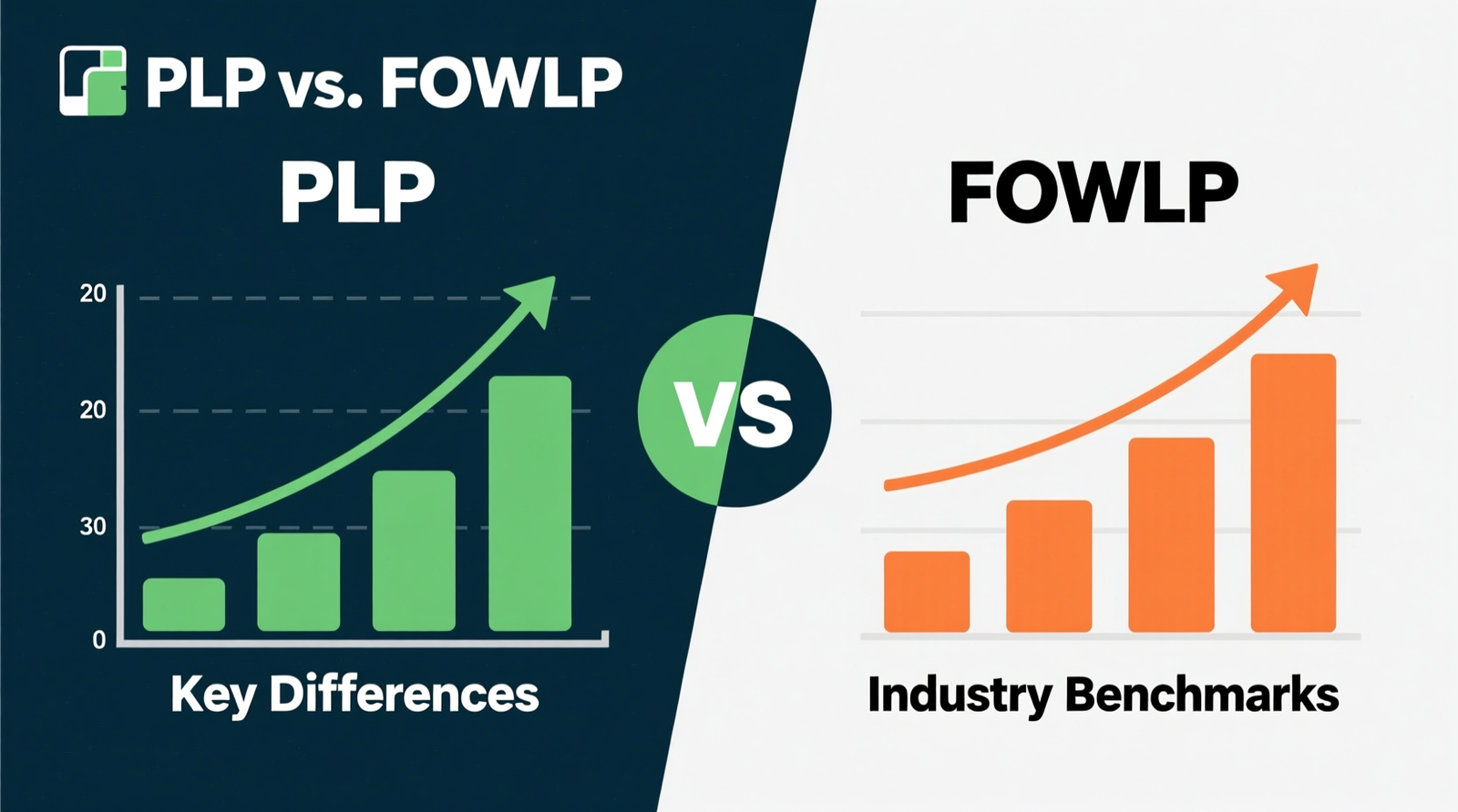
PLP vs. FOWLP: Key Differences and Industry Benchmarks
While both PLP and FOWLP share core principles—such as fan-out redistribution layers and chip-first or chip-last processes—their main difference lies in substrate shape and scalability. FOWLP uses round silicon wafers, which limits the number of dies per batch and material utilization. PLP, on the other hand, uses square or rectangular panels that significantly improve layout efficiency and reduce edge losses.
Compared to Fan-Out Wafer-Level Packaging, Panel-Level Packaging allows a 2–3x increase in production throughput due to larger substrate size, according to reports from Semiconductor Engineering. This makes PLP particularly attractive for Original Equipment Manufacturers (OEMs) and Outsourced Semiconductor Assembly and Test (OSAT) providers seeking to meet market demand for advanced, compact chip packaging at scale.
FOWLP remains dominant in markets that emphasize miniaturization, like mobile and wearable devices. PLP, however, is gaining ground in high-volume sectors such as automotive electronics and 5G base stations where cost efficiency and mass integration matter most.
TL;DR: PLP outscales FOWLP with larger panels for higher yields and layout flexibility, meeting the needs of high-volume and performance-driven industries.
Industry Adoption and Competitor Landscape
Major players in the semiconductor packaging field—including ASE Technology, Amkor Technology, and Samsung Electro-Mechanics—are actively investing in PLP R&D and pilot lines. Samsung, in particular, has been developing next-gen PLP processes for advanced memory and Exynos processors. Amkor’s focus has been to adapt panel packaging for high-efficiency AI and automotive chips.
However, adoption is not without challenges. PLP requires new equipment and processes such as panel-level lithography systems and precision molding tools. Despite these hurdles, companies that lead in PLP adoption stand to gain a competitive advantage in performance-focused markets.
Analysts at Gartner note that PLP adoption will accelerate as demand grows for heterogeneous integration and multi-die systems in areas like edge computing and IoT (Internet of Things). Benchmarking data increasingly shows that panel-based production can reach cost per unit and reliability metrics that outperform older wafer-based methods over time.
TL;DR: Leading semiconductor firms are embracing PLP to meet future demands in AI, automotive, and IoT markets, despite the need for capital investment in new tools and processes.
Challenges and Future Outlook for PLP Technology

Despite the promise of PLP, the technology is still transitioning from pilot lines to full-scale production. Key challenges include panel warpage, uniform mold compound distribution, and achieving high-precision alignment across large panel surfaces. Quality control becomes more difficult as the substrate size grows.
Moreover, standardization is still evolving, and current industry tooling is largely designed for the circular wafer format. To address this, consortia such as the SEMI organization are working to establish cross-industry standards for panel sizes, materials, and equipment compatibility.
As these challenges are addressed—backed by growing demand for ultra-compact and high-performance electronics—PLP is expected to achieve widespread adoption. Forecasts from IDC predict a compound annual growth rate (CAGR) of over 20% in PLP-related segments through 2028.
TL;DR: PLP is on the path to broader adoption, though manufacturing challenges and standardization are critical hurdles still being overcome by industry leaders and collaborative efforts.
FAQ
Q: What is the main difference between PLP and FOWLP?
A: The key difference is the substrate format—PLP uses large rectangular or square panels, while FOWLP uses traditional round wafers. PLP offers better material efficiency, improved scalability, and potentially lower costs in high-volume applications.
Q: Which industries benefit the most from Panel-Level Packaging?
A: Industries such as consumer electronics, automotive, 5G infrastructure, and artificial intelligence (AI) benefit significantly from PLP due to its ability to integrate multiple functions into compact, power-efficient packages.
Q: Is Panel-Level Packaging already in mass production?
A: While several companies have piloted PLP lines, full-scale mass production is still limited and mainly focused on high-performance applications. Broader industrial adoption is expected within the next few years as challenges like warpage and panel uniformity are resolved.
Q: Why is PLP important for AI and data-heavy applications?
A: PLP offers superior electrical characteristics and enables more components to be tightly integrated, which is essential for high-speed processing and low-latency data handling required in AI and HPC systems.
Q: Are there any industry standards for panel sizes in PLP?
A: Standardization for PLP is still developing. Organizations like SEMI are actively working on defining industry guidelines to ensure cross-vendor compatibility for panel dimensions and processing equipment.