DFN and QFN Packages Market Overview
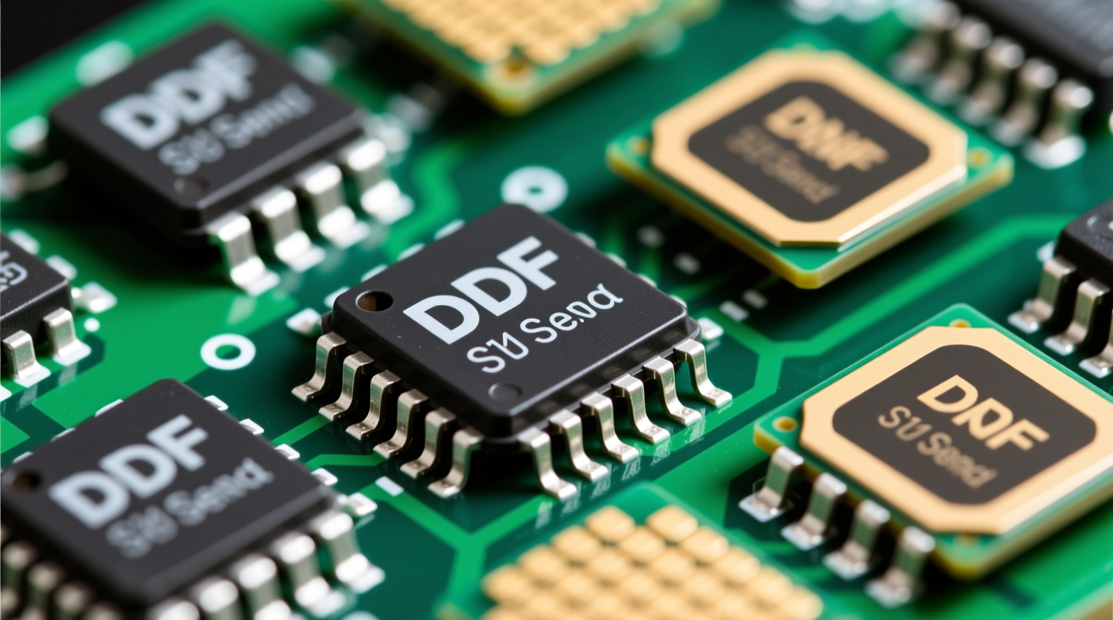
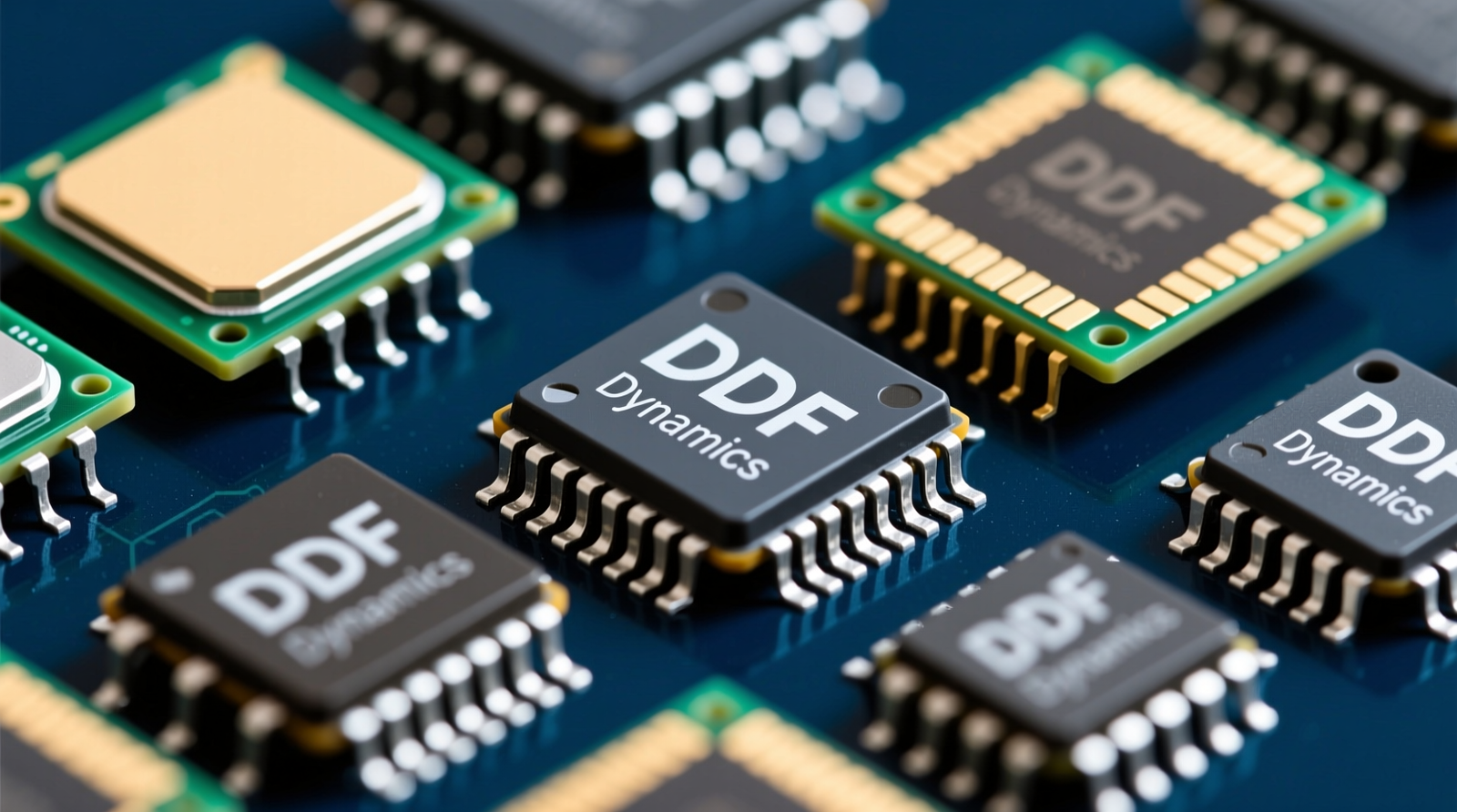
The DFN and QFN packages market is expanding as semiconductor manufacturers and electronics OEMs (original equipment manufacturers) adopt leadless IC (integrated circuit) packaging to enable smaller footprints, better thermal paths, and improved high-frequency electrical performance. DFN stands for Dual Flat No-lead, and QFN stands for Quad Flat No-lead. Both are bottom-terminated components (BTCs), meaning their solderable terminals are on the underside of the package rather than protruding leads.
Resolving the forecast inconsistency: The figures in the original draft reflect two different forecasting baselines commonly seen across third-party research houses (e.g., different definitions of what is included in “DFN/QFN market”—package revenue only vs. package + assembly services; and different base years and scenario assumptions). To keep the narrative coherent and trustworthy, this article uses one primary “base-case” forecast while still acknowledging the alternative view as an “expanded-scope” scenario.
- Base-case (package-focused scope): estimated at USD 5,884.66 million in 2026 and projected to reach USD 7,711.05 million by 2035, implying ~2.9% CAGR (compound annual growth rate) from 2026–2035.
- Expanded-scope scenario (broader revenue capture): some sources cite ~USD 3.4 billion in 2024 rising to ~USD 8.7 billion by 2034 (~9.8% CAGR), typically when including more semiconductor assembly and test value or counting a wider set of leadless package variants.
Methodology note: All market values and growth rates here are aggregated estimates based on a synthesis of public OSAT (Outsourced Semiconductor Assembly and Test) commentary, industry association materials, and third-party packaging market research. Figures are rounded, may vary by source, and should be treated as directional rather than audit-grade.
Why DFN/QFN adoption keeps rising: engineers use these packages for miniaturization and heat removal in power and RF designs. For example, thermal resistance figures such as “<25 °C/W” usually refer to package-to-ambient or junction-to-ambient performance under a defined PCB test condition (board size, copper area, airflow). In practice, DFN/QFN thermal performance depends heavily on exposed pad design, via-in-pad, and copper spreading on the PCB.
These packages are widely used in power management ICs (PMICs), RF front-end modules, automotive radar/ADAS (Advanced Driver-Assistance Systems), and industrial sensors—areas where low parasitics, compact footprints, and robust thermal paths directly translate to system-level performance. For PCB designers, the implication is straightforward: DFN/QFN selection often becomes a layout and thermal design decision as much as a component choice.
External references for fundamentals and compliance: For background on modern packaging ecosystems, see SEMI’s industry resources (https://www.semi.org/en). For restrictions affecting package materials (lead-free, halogen-free adoption drivers), refer to the EU RoHS directive overview (https://environment.ec.europa.eu/topics/waste-and-recycling/rohs-directive_en).
TL;DR: DFN/QFN demand is driven by miniaturization + thermal/RF performance; the article uses the 2026–2035 base-case forecast (2.9% CAGR) while flagging a separate expanded-scope scenario that yields a higher CAGR.
U.S. DFN and QFN Packages Market Snapshot
The U.S. remains strategically important for leadless packaging demand due to strength in automotive electronics, defense, data centers, and AI hardware. This demand is also influenced by policy-driven supply chain localization and incentives aimed at expanding domestic semiconductor capacity.
Across 2023–2025, U.S.-based packaging and electronics manufacturing investments increasingly emphasized QFN for analog, RF, and power devices where tight footprints and predictable electrical behavior are required. Wettable flank QFN—an automotive-oriented variant designed to make solder fillets visible for inspection—has gained traction as reliability requirements tighten.
For OSATs and packaging engineers, the practical investment areas in the U.S. tend to cluster around:
- Automated inspection (AOI: automated optical inspection; plus X-ray for hidden joints)
- High-throughput placement optimized for thin BTC handling
- Automotive-grade process control aligned with near-zero-defect expectations
External reference: For context on U.S. manufacturing policy and incentive direction, see the U.S. Department of Commerce CHIPS program hub (https://www.chips.gov/).
TL;DR: U.S. demand is pulled by automotive/defense/AI; the main packaging upside is in high-reliability QFN variants and the inspection automation needed to support them.
Key Market Findings (Prioritized Insights)
The DFN/QFN ecosystem is evolving fastest where power density and frequency are rising—EV power electronics, 5G RF, and compact AI/edge systems. Instead of listing every statistic, the most decision-relevant signals are summarized below.
- Leadless IC packaging is becoming a default choice for compact power and RF designs due to low parasitics and exposed-pad thermal paths.
- Automotive-grade requirements (inspectability, solder joint robustness, defect control) are accelerating adoption of wettable flank QFN and more rigorous inspection flows.
- Manufacturing capability is a gating factor: facilities without advanced X-ray/AOI and warpage control typically scale DFN/QFN more slowly than top-tier lines.
- Asia-Pacific leads in volume due to dense OSAT capacity, while North America/Europe often drive higher-value, automotive and compute-focused demand.
By-the-numbers (kept concise):
| Item | Base-case | Expanded-scope scenario |
|---|---|---|
| Market value (start year) | USD 5,884.66M (2026) | USD 3.4B (2024) |
| Market value (end year) | USD 7,711.05M (2035) | USD 8.7B (2034) |
| CAGR / period | ~2.9% (2026–2035) | ~9.8% (2024–2034) |
| Why different? | Narrower package-focused scope | Broader scope and/or more aggressive growth assumptions |
TL;DR: The biggest takeaways are (1) DFN/QFN is structurally advantaged for compact power/RF, and (2) market growth rates vary mainly due to scope and forecast assumptions, not because the underlying adoption trend is in doubt.
Latest Trends in Leadless IC Packaging (DFN/QFN)
DFN and QFN market momentum is tied to three engineering trends: higher switching currents in compact power stages, higher RF frequencies (including mmWave, millimeter wave), and thinner end products that constrain z-height.
1) Ultra-thin packages: The push toward sub-0.8 mm package heights is strongest in smartphones, wearables, and space-constrained industrial nodes. Thinner packages improve mechanical stacking flexibility but also tighten process windows for warpage control and solder void management.
2) Wettable flank QFN for automotive: Automotive electronics increasingly expects inspectable joints. Wettable flanks create a visible side fillet after reflow, enabling AOI (automated optical inspection) to catch defects that would otherwise require X-ray. This is particularly relevant for ADAS and under-hood modules with harsh temperature cycling.
3) Copper clip vs. wire bond: Copper clip interconnects (instead of fine wire bonds) are used to reduce electrical resistance/inductance and improve heat spreading. Claims such as “lower thermal resistance” are typically measured relative to a baseline wire-bond QFN of comparable body size, on a defined thermal test board.
External reference: For practical background on SMT (surface-mount technology) assembly considerations that affect BTC reliability (stencil design, reflow, inspection), see the IPC (Association Connecting Electronics Industries) home page and standards hub (https://www.ipc.org/).
TL;DR: The market’s technology roadmap is being shaped by ultra-thin form factors, automotive inspectability (wettable flanks), and copper-clip power packaging for better electrical/thermal performance.
DFN and QFN Packages Market Dynamics
Market dynamics for DFN/QFN are best understood as a push-pull between performance needs (drivers), manufacturing realities (restraints), growth vectors (opportunities), and supply-side friction (challenges).
Driver: Miniaturization and performance density in automotive and consumer electronics
As OEMs compress PCB area while increasing functionality, leadless packages gain share because they deliver shorter electrical paths and a highly usable exposed thermal pad. In RF and fast-switching power circuits, lower parasitic inductance typically improves ringing/EMI behavior compared with many leaded alternatives, especially when the PCB layout is optimized.
Practical implication: For PCB designers, DFN/QFN adoption usually means prioritizing thermal pad/via design, solder paste coverage, and a clear inspection strategy (AOI + X-ray where needed) early in the layout stage.
TL;DR: Miniaturization plus power/RF performance requirements are structural tailwinds for DFN/QFN, directly supporting market growth in high-density electronics.
Restraint: Manufacturing complexity and solder joint reliability (BTC reality)
DFN/QFN are bottom-terminated, so solder joints are partially hidden and more sensitive to process setup. Typical pain points include voiding under the exposed pad, coplanarity on very thin bodies, and thermal cycling fatigue—especially in automotive environments.
What this means operationally: assemblers often need better paste printing control, tighter placement tolerances, and more frequent use of X-ray inspection than with leaded packages. Those upgrades raise capital intensity and slow adoption for smaller lines.
TL;DR: DFN/QFN can be harder to assemble and inspect; facilities that can’t justify X-ray/AOI upgrades tend to scale more slowly, moderating growth in some tiers.
Opportunity: EV electrification, AI infrastructure, and IoT device proliferation
EVs expand demand for compact, thermally robust power management and sensing; AI infrastructure increases high-current power stages and thermal density; IoT growth keeps pressure on ultra-small footprints and low power loss.
Where opportunity concentrates:
- EV battery management and onboard charging: power ICs, gate drivers, sensing
- Edge AI compute: compact PMICs and power stages close to processors
- Industrial IoT: tiny sensors and connectivity modules where board space is premium
External reference: For a neutral macro view of connected device scale (used widely as an industry talking point), see ITU (International Telecommunication Union) resources on IoT and connectivity (https://www.itu.int/).
TL;DR: EV + AI + IoT creates multi-end-market pull for DFN/QFN, particularly in power and sensing, supporting long-run demand even when consumer cycles fluctuate.
Challenge: Supply chain volatility and rising material/equipment costs
Material inputs (leadframes, copper, molding compound) and capital equipment lead times can swing cost and availability. When substrate/leadframe supply tightens, OSATs may prioritize higher-margin programs, which can affect lead times for commodity DFN/QFN.
Strategy implication: For procurement and engineering managers, dual sourcing (where possible), package alternates (pin-compatible), and early capacity reservations reduce schedule risk—particularly for automotive programs with strict PPAP-style expectations (Production Part Approval Process, commonly used in automotive supply chains).
TL;DR: Cost inflation and lead-time risk can constrain near-term output; resilient sourcing strategy becomes part of “package selection” in practice.
Segmentation Analysis
Segmentation is most useful when it connects package choice to real design constraints: pin count, thermal path, EMI behavior, assembly yield, and inspection needs.
By Type: QFN vs. DFN package characteristics
QFN (Quad Flat No-lead): Typically selected when designs need higher I/O counts, good grounding, and strong RF/power performance. Common industry body sizes include 3×3 mm, 4×4 mm, 5×5 mm, and larger multi-row variants; QFN is frequently specified for RF front-end parts, transceivers, interface ICs, and mid-power PMICs.
DFN (Dual Flat No-lead): Often preferred for smaller, simpler pin-count devices—especially discrete-like ICs (LDOs: low-dropout regulators; small DC–DC converters; LED drivers; sensors). DFN footprints such as 2×2 mm and 3×3 mm are common where board area is extremely constrained.
DFN vs QFN package advantages in automotive: QFN is frequently used for modules needing more I/Os and RF grounding (e.g., radar-related devices), while DFN is a frequent choice for compact power and sensing devices. Automotive programs increasingly specify wettable flank options for improved inspection confidence.
TL;DR: QFN tends to win when pin count/RF grounding matters; DFN is a go-to for compact power and sensing. Automotive pushes both toward wettable flanks and stricter inspection flows.
By Application: where DFN/QFN deliver the most value
Automotive: Growth is driven by EV power electronics, ADAS, radar, and in-cabin connectivity. Key automotive use cases include:
- Battery management ICs and cell monitoring
- Onboard chargers and DC–DC converters
- Radar and sensor interface ICs
- Body electronics and gateway modules
Takeaway for automotive engineers: prioritize wettable flank availability, MSL (Moisture Sensitivity Level) handling requirements, and thermal cycling performance when choosing DFN/QFN for safety-relevant electronics.
Consumer electronics: Smartphones, wearables, and gaming devices pull demand for ultra-thin QFN/DFN. Here, z-height and RF integrity (plus fast-charging thermals) are key selection criteria.
Industrial: Industrial automation emphasizes reliability under vibration and temperature extremes. Main industrial subsegments include sensors, PLCs (programmable logic controllers), motor drives, and industrial gateways.
Communication infrastructure: 5G RF chains and high-speed connectivity benefit from QFN’s low parasitics and grounding options. Designs also depend heavily on PCB stack-up and grounding strategy, so “package advantage” is realized only when layout is executed correctly.
Others (medical, aerospace/defense, renewable energy): These segments value reliability, traceability, and long lifetimes. DFN/QFN selection is often constrained by qualification requirements and supply continuity.
TL;DR: Automotive and communications reward DFN/QFN for thermal/RF performance; consumer pushes ultra-thin formats; industrial and medical emphasize reliability and qualification discipline.
Regional Outlook (DFN and QFN Market Growth by Geography)
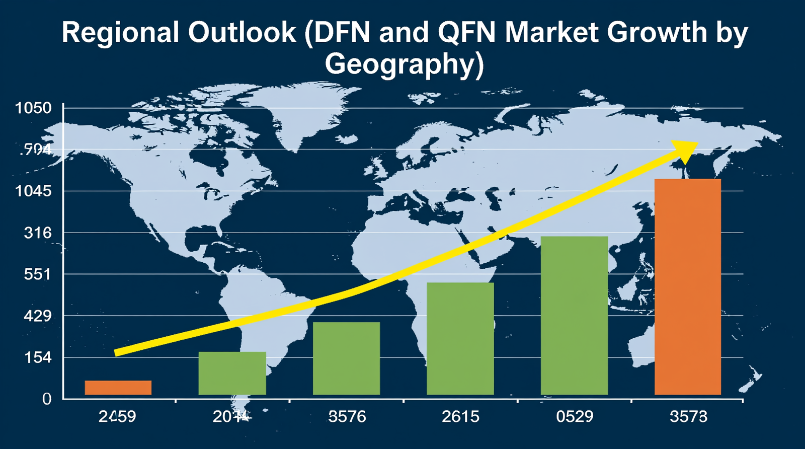
Regional differences are mainly about where assembly capacity sits and which end markets dominate—volume consumer manufacturing vs. high-value automotive/compute.
North America
North America is driven by high-value applications (automotive electronics, defense, data centers, and AI). The region’s packaging focus often tilts toward tighter quality systems, advanced inspection, and automotive-grade variants.
TL;DR: North America is less about volume dominance and more about high-value, high-reliability DFN/QFN demand—especially automotive and AI infrastructure.
Europe
Europe’s DFN/QFN demand correlates strongly with automotive production, industrial automation, and renewable energy power electronics. Automotive-grade reliability expectations also increase demand for inspectable QFN variants and robust process control.
TL;DR: Europe is anchored by automotive and industrial; DFN/QFN demand follows qualification-heavy, reliability-first buying patterns.
Asia-Pacific (DFN and QFN market growth in Asia-Pacific)
Asia-Pacific leads in DFN/QFN volume because it hosts the densest concentration of OSAT capacity and electronics manufacturing ecosystems. This concentration shortens supply chains for consumer electronics and also supports large-scale automotive and industrial growth.
TL;DR: Asia-Pacific is the volume engine for DFN/QFN due to OSAT scale and integrated electronics manufacturing ecosystems.
Middle East & Africa
Middle East & Africa remains smaller in packaging operations but grows through infrastructure build-outs (5G, data centers), industrial projects, and renewable energy deployments—pulling in DFN/QFN-based electronics via imports and contract manufacturing.
TL;DR: MEA growth is infrastructure-led; demand increases mainly through imported electronics and expanding industrial/telecom deployments.
Leading DFN and QFN Packages Companies (OSAT and Assembly Ecosystem)
The competitive landscape is shaped by OSAT scale, automotive qualification capability, and advanced process tooling (molding, singulation, copper clip attach, AOI/X-ray). Key OSAT players commonly referenced in DFN/QFN supply chains include:
- ASE
- Amkor Technology
- JCET
- Powertech Technology Inc.
- Tongfu Microelectronics
- Tianshui Huatian Technology
- UTAC Group
- ChipMOS Technologies
- King Yuan Electronics
Source-basis note: Company-level positioning discussed in public markets is typically derived from annual reports, earnings commentary, and industry briefings rather than standardized, apples-to-apples “DFN/QFN-only” revenue reporting.
TL;DR: DFN/QFN supply is concentrated among large OSATs; differentiation comes from automotive qualification readiness, inspection capability, and advanced interconnect options like copper clip.
Investment Analysis and Market Opportunities

Investment in DFN/QFN capacity tends to follow three triggers: EV ramp, AI/data-center power density, and packaging automation requirements. In practice, capital often goes first to inspection and yield-enabling steps because BTC assembly is less forgiving than many leaded packages.
Where investment is most actionable:
- Automation: faster placement and tighter process controls for thin packages
- Inspection: AOI + X-ray to manage hidden solder joints
- Power packaging upgrades: copper clip lines and enhanced leadframe designs
TL;DR: The best-capitalized opportunities cluster around automation, inspection, and power-focused QFN/DFN variants that unlock higher density and reliability.
New Product Development and Technology Roadmap
Product development in DFN/QFN increasingly focuses on manufacturability and reliability, not just shrinking the outline. The most common roadmap themes include:
- Ultra-thin constructions for mobile and wearables
- Wettable flank designs for automotive inspection requirements
- Copper clip interconnects to reduce electrical loss and improve thermal spreading
- Material upgrades aligned with environmental compliance and high-frequency performance needs
External reference: For environmental regulation drivers affecting electronics materials, see the EU REACH overview (https://environment.ec.europa.eu/topics/chemicals/reach-regulation_en).
TL;DR: The roadmap is dominated by thinner profiles, better inspectability, and higher-current interconnects—because reliability and yield are now as important as size.
Recent Industry Developments

- Capacity expansions: Additional QFN/DFN lines continue to be added where automotive and compute demand justify inspection and automation investments.
- Automotive packaging upgrades: Wettable flank introductions and inspection enhancements remain a recurring theme as OEMs push for more robust solder joint verification.
- Manufacturing analytics: AI-assisted inspection is increasingly deployed to improve detection of voiding, misalignment, and subtle assembly defects in thin BTCs.
TL;DR: The most meaningful “news” is incremental but important—capacity, inspectability, and inspection automation are the levers shaping near-term competitiveness.
Report Coverage and Market Scope
Most DFN/QFN market studies segment by type (DFN vs QFN), end use (automotive, consumer, industrial, communication, others), and region. However, the single biggest reason reports disagree is scope definition—what counts as DFN/QFN (and whether revenue is attributed to package sales alone or includes broader assembly/test value).
How to interpret forecasts responsibly: Use the CAGR and market size that matches your decision. A PCB design team might care more about adoption and availability by package code, while an investor may prefer a broader “packaging services captured” view that yields a higher growth rate.
TL;DR: DFN/QFN reports can differ materially because “market scope” differs; always match the forecast to the business decision you’re making.
Market Summary and Outlook

DFN and QFN packages are foundational to modern electronics because they balance size, thermal performance, and electrical behavior better than many leaded alternatives. Adoption is most durable in automotive electrification, RF connectivity (including 5G), industrial sensing, and increasingly power-dense compute platforms.
Near-term constraints come from assembly complexity, inspection needs, and supply chain variability, but ongoing innovation—wettable flanks, copper clip, ultra-thin formats, and stronger inspection automation—continues to reduce practical barriers to adoption.
TL;DR: DFN/QFN remains a resilient growth market because it solves real packaging problems (thermal/RF/size), and process innovations are steadily expanding where and how these packages can be deployed.
FAQ
Q: What is the difference between DFN and QFN packages?
A: DFN (Dual Flat No-lead) typically has terminals on two sides and is often used for smaller pin-count devices like regulators, sensors, and compact power ICs. QFN (Quad Flat No-lead) has terminals on all four sides, making it better suited for higher I/O count devices and many RF applications where grounding and signal integrity are critical.
Q: When should designers choose DFN vs QFN for automotive electronics?
A: Choose QFN when you need higher pin count, strong grounding for RF/noise control, or standardized automotive-qualified options (including wettable flank versions). Choose DFN for compact power and sensing devices where low profile and minimal footprint matter most. In both cases, validate thermal performance on your actual PCB stack-up and confirm inspection strategy (AOI/X-ray) early.
Q: What PCB design guidelines are critical for DFN/QFN reliability?
A: Key items include correct exposed-pad solder paste coverage (often segmented to reduce voiding), thermal via arrays under the exposed pad, copper spreading for heat, and clear solder mask definition. Also plan for inspection: bottom-terminated joints may require X-ray, and automotive designs often prefer wettable flank QFNs to make solder fillets visible to AOI.
Q: How do DFN and QFN packages affect BOM cost and supply chain risk versus BGA or leaded packages?
A: DFN/QFN can reduce PCB area and sometimes lower total system cost, but they may increase assembly and inspection costs (X-ray/AOI) compared with leaded packages. Versus BGA (Ball Grid Array), DFN/QFN can be simpler at moderate I/O counts, but supply risk depends on how many qualified sources offer the same footprint and automotive grade. For risk control, prioritize second-source footprints and verify OSAT capacity/qualification for your required variant (e.g., wettable flank).
Q: Why do different reports show very different DFN/QFN market sizes and CAGRs?
A: The most common reason is different market definitions and revenue capture. Some reports count only DFN/QFN package revenue, while others include broader assembly/test services or a wider set of leadless package variants. Different base years and scenario assumptions (base vs optimistic) can also change the CAGR materially.