Executive summary for power electronics OEMs, packaging engineers, materials suppliers, and investors: This article explains what’s changing in power module packaging technologies between 2026 and 2031—especially for automotive SiC power module packaging, double-sided cooled power module design, and advanced ceramic substrate for EV inverters. It covers forecast context, packaging architectures (interconnects, substrates, die attach), reliability tests, regional demand hotspots, and practical barriers to scale.
- Growth outlook: Packaging value growth is tied less to “more modules” and more to more demanding module designs (higher voltage, higher temperature, lower inductance, longer lifetime).
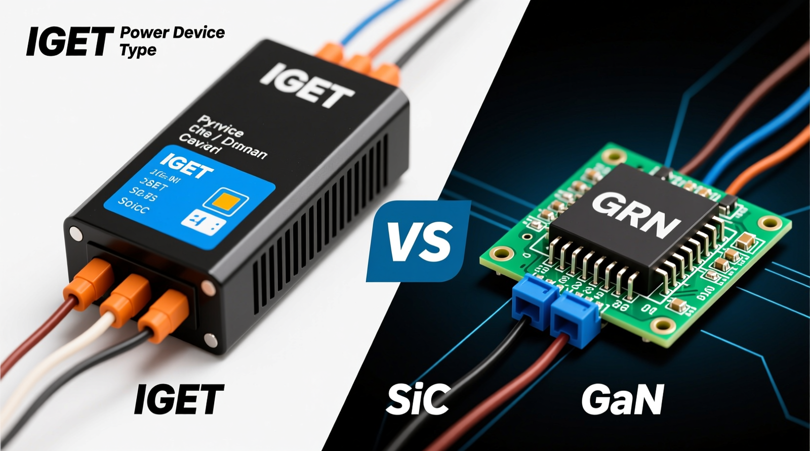
- Primary technology shift: Migration from silicon IGBT (Insulated Gate Bipolar Transistor) modules toward wide-bandgap (WBG) devices—SiC (silicon carbide) and GaN (gallium nitride)—forces new substrate, interconnect, and thermal stack choices.
- Top strategic implications: (1) qualify materials for higher junction temperature (Tj) operation, (2) invest in low-inductance interconnect + insulation design for 800 V-class systems, (3) build reliability test capacity (power cycling/thermal cycling/HTRB) early to avoid late-stage automotive delays.
TL;DR: Power module packaging is becoming an engineering differentiator—thermal + inductance + reliability are now the main levers for performance and cost.
Introduction

Power module packaging is the set of materials and mechanical/electrical structures that mount and interconnect power semiconductor dies (chips), deliver electrical insulation, and remove heat. It directly affects switching behavior (via parasitic inductance), thermal limits (via thermal resistance), and lifetime (via thermo-mechanical stress).
From 2026–2031, the packaging conversation is increasingly about how you package WBG devices—not just whether you use them. That includes ceramic substrate selection (e.g., DBC—Direct Bonded Copper), die attach (e.g., sintered silver), and interconnect style (wire vs ribbon vs planar).
TL;DR: Packaging is no longer “back-end”—it sets inverter efficiency, size, and durability in EV, industrial, renewables, and data center power.
Market Overview and Growth Forecast (2026–2031)
Representative industry market models project the power module packaging market at ~USD 3.01B in 2026 (up from ~USD 2.74B in 2025) and ~USD 4.78B by 2031, implying a ~9.72% CAGR over 2026–2031. These figures should be read as value-based estimates (USD revenue) rather than unit volume, and are typically derived from a blended approach: device shipment forecasts, module bill-of-materials (BOM) assumptions, and regional production splits.
What’s materially driving value growth is the rising share of packaging content per module: higher-performance substrates, advanced die attach, and more complex cooling/interconnect stacks—especially in automotive and grid-tied converters.
TL;DR: Most of the “market growth” is packaging content and complexity growth, not just more units.
Packaging-Centric Technology Trends (What Engineers Actually Change)
Wide-Bandgap (WBG) Devices: SiC and GaN vs IGBT—Packaging Implications
WBG devices raise the bar on packaging. SiC MOSFETs (metal-oxide-semiconductor field-effect transistors) are commonly used in 650 V to 1200 V (and higher) automotive traction and fast-charging applications; GaN is widely used around 100–650 V in high-frequency power conversion. IGBTs still dominate many cost-sensitive high-power systems, but their lower switching speed and higher losses push designers to larger magnetics/cooling.
Range improvement claims (often cited as ~5–10% for SiC inverters versus silicon IGBT baselines) depend strongly on drive cycle, inverter switching strategy, and thermal limits. These numbers are consistent with industry benchmarks and representative OEM disclosures, but they are not universal and can be lower if the baseline system is already highly optimized.
Comparison table (SiC vs GaN vs IGBT in packaging context):
| Device | Typical voltage range (common use) | Typical switching frequency | Typical applications | Packaging challenges (common) |
|---|---|---|---|---|
| IGBT | 600–1700 V (and higher in traction/grid) | ~2–20 kHz (often) | Industrial drives, rail traction, legacy EV platforms, grid converters | High thermal cycling stress, larger thermal stack; inductance less critical than WBG but still relevant |
| SiC MOSFET | 650–1200 V (common), extending upward | ~10–100+ kHz (use-case dependent) | EV traction inverters (800 V-class), fast chargers, solar/string inverters | Needs low-inductance layouts; higher Tj targets push die attach/substrate reliability; partial discharge/insulation at higher dv/dt |
| GaN (HEMT) | 100–650 V (common) | ~100 kHz to MHz-class (application dependent) | Onboard chargers, DC-DC, data center PSUs, telecom rectifiers, fast chargers | Very fast switching makes loop inductance/EMI critical; package parasitics and gate loop design dominate performance |
For authoritative background on SiC and GaN fundamentals and application positioning, see materials from IEEE (Institute of Electrical and Electronics Engineers) and leading device manufacturers’ application notes (e.g., IEEE Xplore for peer-reviewed papers; and Wolfspeed Knowledge Center for SiC application resources).
TL;DR: WBG devices make packaging parasitics, insulation, and high-temperature materials the limiting factors—not the silicon itself.
800 V EV Platforms and High dv/dt Insulation Design
The shift toward 800 V-class EV architectures (higher bus voltage to reduce current for the same power) tightens packaging requirements around insulation coordination and high slew rates (dv/dt). Faster switching can raise electric field stress, increasing risk of partial discharge (localized dielectric breakdown) if creepage/clearance and material selection are marginal.
For context on functional safety and automotive electronics development constraints, standards such as ISO 26262 (road vehicles—functional safety) shape design verification expectations, while automotive qualification practices are commonly aligned to AEC documents (Automotive Electronics Council). While AEC specifications are distributed via AEC directly, a practical overview is available through multiple semiconductor vendors’ qualification guides.
TL;DR: 800 V pushes packaging toward stronger insulation design and lower inductance layouts to manage dv/dt, EMI, and discharge risk.
Advanced Power Module Packaging: Interconnect Styles and Why They Matter
As switching speeds rise, the interconnect choice becomes a performance knob:
- Wire bonding: Traditional aluminum (Al) wire bonds are mature and cost-effective, but they add loop inductance and can be a wear-out mechanism under power cycling (bond heel cracks, lift-off).
- Ribbon bonding: Wider Al ribbons reduce resistance and inductance versus round wire, improving current handling and lowering switching overshoot; they can also improve thermo-mechanical robustness, depending on geometry and attachment quality.
- Planar interconnect (e.g., copper clips, leadframes, or planar bus structures): Minimizes loop inductance and improves current spreading; often paired with low-inductance module layouts for WBG. The trade-off is process complexity and managing stress at interfaces.
In practical automotive SiC power module packaging, designers often combine planar or ribbon interconnects with a laminated busbar approach to control stray inductance in both the power loop and the gate loop.
TL;DR: Moving from wire to ribbon/planar interconnect is one of the most direct ways to cut inductance and improve WBG switching stability and reliability.
Thermal Metrics, Cooling Architectures, and Realistic Targets

Thermal design is typically discussed using:
- Tj (junction temperature): the semiconductor junction operating temperature. Silicon IGBT systems often target lower Tj; SiC devices can be specified for higher Tj (commonly discussed in the ~175–200°C class depending on device and mission profile), but packaging materials must survive the same environment.
- Rth (thermal resistance): temperature rise per watt (e.g., junction-to-case). Lower Rth enables more power or smaller cooling.
A common engineering lever is double-sided cooling (extracting heat from both sides of the die). In representative module studies, double-sided cooling can reduce effective thermal resistance meaningfully versus single-sided approaches by removing a bottleneck interface and increasing heat spreading area; the exact improvement depends on the baseline stack, coolant approach, and die size. In EV traction inverter discussions, it’s not unusual to target a step-change in thermal path performance to unlock higher continuous power without over-sizing the cold plate.
For background on thermal management concepts and power electronics cooling methods, NREL (National Renewable Energy Laboratory) and other public research organizations provide useful reference material (e.g., NREL).
TL;DR: Tj capability is only useful if the package can remove heat and survive stress—double-sided cooling is a major path to lower Rth in high-density modules.
Reliability: Stress Tests Packaging Must Pass
Power modules are judged by how they age under repeating stress, not just peak performance. Common reliability evaluations include:
- Power cycling: repeated electrical loading heats and cools the die and interconnects, stressing bond wires/ribbons, die attach, and metallization.
- Thermal cycling: environmental temperature swings stress mismatched coefficients of thermal expansion (CTE) across ceramics, copper, solders, and encapsulants.
- HTRB (High-Temperature Reverse Bias): a high-temperature electrical stress used to evaluate leakage and stability under reverse bias, influenced by insulation design, contamination control, and electric field management.
Packaging decisions directly influence these outcomes. Example: switching from solder to sintered silver die attach can improve high-temperature capability and reduce fatigue in some regimes, while replacing wire bonds with planar interconnect can reduce bond-related failure modes—though each change introduces its own process-control requirements.
TL;DR: The “best” package is the one that survives power cycling, thermal cycling, and HTRB with margin—materials and interconnect choices decide that outcome.
Applications & Use Cases (Where Packaging Choices Show Up)

- EV traction inverters (800 V-class): A typical SiC module architecture uses DBC substrates (often AlN—aluminum nitride—for higher thermal conductivity), low-inductance power loops, and increasingly baseplate-less or optimized baseplate stacks to reduce thermal interfaces.
- Onboard chargers and DC-DC converters: GaN-based designs often prioritize ultra-low inductance and EMI control; packaging parasitics can dictate achievable switching frequency and filter size.
- Industrial motor drives (VSDs): VSD stands for variable speed drive. Packaging must balance cost, long duty cycles, and ruggedness; upgrading interconnect and TIM (thermal interface material) selection can raise power density without sacrificing lifetime.
- Renewables and grid-tied inverters: High-voltage insulation integrity and lifetime under thermal cycling are central; packaging design often emphasizes robust substrate systems and conservative insulation margins.
- Data center power (high-efficiency PSUs): High-frequency switching pushes low-inductance packaging and thermal spreading; compact form factors raise the stakes on TIM selection and hotspot control.
Two concrete, anonymized examples seen in the field:
- OEM A (automotive): A move from wire-bonded IGBT modules to a low-inductance SiC module with ribbon/planar interconnect reduced switching overshoot and enabled higher switching frequency, allowing smaller passive components in the inverter stage (at the cost of tighter process control and EMI validation effort).
- OEM B (industrial): An industrial drive supplier adopted an advanced ceramic substrate stack and upgraded TIM to reduce case temperature at the same load, improving thermal margin for harsh ambient installations and extending service intervals.
TL;DR: Packaging decisions are application-specific: EV needs low inductance + high power density; renewables need insulation + lifetime; data centers need high-frequency parasitic control.
Market Challenges and Investment Barriers (with Mitigation)
-
Capital intensity: Advanced module lines (sintering, precision attach, inspection, reliability labs) require high upfront spend.
Mitigation: Partner with experienced OSATs (Outsourced Semiconductor Assembly and Test) for ramp, or phase investment by outsourcing pilot builds while internalizing high-volume later. -
Qualification time and reliability risk: Automotive-grade releases demand extended validation and traceability.
Mitigation: Build reliability test vehicles early (power cycling/thermal cycling/HTRB), and co-develop with key material suppliers to stabilize process windows. -
Supply chain concentration (substrates, metallization, high-end TIMs): Shortages or quality variation can stall ramps.
Mitigation: Dual-source critical materials, lock specs with suppliers, and use incoming inspection/metrology to detect lot-to-lot drift. -
Regional manufacturing gaps: Emerging regions may lack deep ecosystems for ceramics, metallization, and high-reliability assembly.
Mitigation: Leverage government incentive programs where applicable (e.g., U.S. CHIPS and Science Act reference) and structure JVs with established packaging clusters.
TL;DR: The biggest barriers are capex + qualification; the fastest mitigations are OSAT partnerships, early reliability engineering, and co-development with substrate/material suppliers.
Segment Analysis (Engineering-Relevant View)
By Component: Substrates, Die Attach, Interconnect, TIM
Power module packaging BOM typically includes substrate, die attach, interconnect, encapsulant/gel, baseplate (optional), and TIM. Substrates were estimated at ~27.85% of 2025 market revenue (value share, not unit share) in the provided dataset; expect that share to remain structurally high through 2031 as WBG adoption increases ceramic performance requirements—even if pricing pressure moderates the percentage.
- Substrates: DBC on AlN (aluminum nitride) is often chosen for high thermal conductivity; Al2O3 (alumina) remains cost-effective for many segments. Substrate selection affects thermal spreading, insulation, and CTE mismatch behavior.
- Die attach: Sintered silver is increasingly used for high-temperature, high-reliability SiC modules; advanced solders remain common where cost and process simplicity dominate.
- Interconnect: Moving to ribbon/planar reduces inductance and can shift failure modes away from bond wires—often critical for fast-switching WBG devices.
- TIM: Advanced TIMs (gap fillers, phase-change, high-k greases) reduce interface losses; quality and pump-out resistance matter for long life.
TL;DR: Substrate + die attach + interconnect are the “big three” performance levers; TIM quality often decides whether the design meets thermal targets in the real vehicle/system.
By Power Device Type: IGBT vs SiC vs GaN
IGBT packaging remains significant in mature industrial and traction segments where switching frequency is modest and cost per kW is tightly managed. SiC is the fastest-growing driver for advanced power module packaging because it pushes higher dv/dt, higher operating temperature ambitions, and lower inductance needs. GaN packaging growth concentrates in high-frequency conversion (telecom/data center/fast chargers) where parasitic reduction is a first-order requirement.
TL;DR: IGBT volumes persist, but SiC/GaN disproportionately drive advanced packaging content and process innovation.
Geographic Analysis (with Application Hotspots)
Asia-Pacific
Asia-Pacific leads in packaging scale and ecosystem depth (ceramics, assembly, test). China in particular is a hotspot for EV traction inverters and fast-charging infrastructure buildout; Japan and South Korea remain strong in automotive supply chains and materials; Southeast Asia continues to attract OSAT and electronics manufacturing investment.
TL;DR: Asia-Pacific combines demand (EV/industrial) with the most complete packaging supply chain.
North America
North America’s demand is closely tied to EV adoption, data center power growth, and grid modernization. Domestic capacity expansion is influenced by policy and incentives (see CHIPS Act reference above) and by efforts to shorten supply chains for strategic components.
TL;DR: North America is capacity-building around EV + data centers, with incentives shaping where packaging investments land.
Europe
Europe is a focal region for automotive-grade SiC modules and high-efficiency industrial automation, with strong emphasis on qualification rigor and lifecycle traceability. The region’s energy transition also supports demand for renewable and grid conversion hardware.
TL;DR: Europe’s differentiator is automotive-grade qualification depth and high-efficiency industrial adoption.
Middle East and Africa
The Middle East shows growing pull from utility-scale solar/wind and grid infrastructure—applications that favor high-voltage insulation integrity and conservative reliability margins. Local manufacturing depth varies widely; many projects source modules internationally while building regional system integration capability.
TL;DR: Demand is project-driven (renewables/grid), with packaging needs centered on high voltage and long lifetime.
Competitive Landscape

Competition in power module packaging is less about “who has a module” and more about who can repeatedly deliver: (1) low-inductance designs at scale, (2) stable substrate and die attach quality, and (3) proven reliability results under standardized stress tests. Leading device makers, module houses, materials suppliers, and OSATs compete and collaborate across these layers.
TL;DR: Sustainable advantage comes from process control + reliability validation, not just a single clever package concept.
Research Scope and Methodology (Data Transparency)
The referenced forecast period is 2026–2031 with a 2025 base year and a 2026 starting estimate. Typical market sizing methodology combines:
- Secondary research: public financials, trade data, government policy documents, technical publications, and supplier/OEM announcements.
- Primary inputs (where available): interviews with module makers, materials suppliers, and packaging/assembly stakeholders to validate BOM splits and adoption curves.
- Forecast model: usually a bottom-up build (device shipments × module content assumptions) reconciled with top-down constraints (regional manufacturing capacity, end-market production, and ASP trends).
When interpreting segment shares (e.g., substrates at 27.85% in 2025), confirm whether the share is by value (revenue) or volume (units); value shares can rise even if unit shares stay flat due to premium materials (e.g., AlN, thick copper, advanced metallization).
TL;DR: Treat all percentages as model-dependent; the most reliable signal is the direction of technology shift (WBG + higher-performance substrates/interconnect/cooling).
Market Opportunities and Future Outlook (2026–2031)

- Automotive SiC power module packaging: More OEMs will standardize low-inductance layouts, higher-Tj-capable attach, and stricter insulation design as 800 V platforms scale.
- Double-sided cooled power module design: Expect more adoption where continuous power and footprint are constrained (performance EVs, commercial EVs, high-density industrial drives).
- Advanced ceramic substrate for EV inverters: Continued pull for higher thermal conductivity ceramics and robust metallization to manage cycling fatigue.
- OSAT and ecosystem partnerships: Packaging capability increasingly sits across a network—materials, ceramics, assembly, test—making co-development a differentiator.
TL;DR: The biggest “opportunity” is delivering manufacturable, qualified, low-inductance and thermally efficient packages—not just adopting SiC/GaN devices.
FAQ
Q: What is automotive SiC power module packaging, and how is it different from IGBT module packaging?
A: Automotive SiC power module packaging is optimized for fast switching (high dv/dt), low parasitic inductance, higher temperature capability, and strict reliability requirements. Compared with many IGBT modules, SiC modules more often use low-inductance interconnects (ribbon/planar), higher-performance ceramic substrates, and advanced die attach (e.g., sintered silver) to maintain efficiency and lifetime under power cycling.
Q: What does “double-sided cooled power module design” mean in practice?
A: It means heat is extracted from both sides of the semiconductor die or module stack instead of primarily through one side into a baseplate/cold plate. This can reduce effective thermal resistance (Rth) and hotspot temperature, enabling higher continuous power density—provided the mechanical stack-up and insulation are designed to handle stress and manufacturability.
Q: Which reliability tests most often limit advanced power module packaging designs?
A: Power cycling and thermal cycling commonly expose interconnect and die-attach fatigue, while HTRB (High-Temperature Reverse Bias) stresses insulation cleanliness and electric-field design. Packaging choices—wire vs planar interconnect, solder vs sintered attach, substrate material, and encapsulation—directly influence outcomes in these tests.
Q: How do advanced ceramic substrate choices (AlN vs alumina) affect EV inverter packaging?
A: AlN (aluminum nitride) generally offers higher thermal conductivity than alumina, improving heat spreading and thermal margins, which can support higher power density. Alumina is often lower cost and widely used when thermal requirements are less aggressive. The right choice depends on inverter power, cooling system, duty cycle, and cost targets.
Q: What are the biggest practical barriers to scaling advanced power module packaging production?
A: The main barriers are capex for specialized processes (precision attach, sintering, inspection), long qualification timelines (especially automotive), and supply chain constraints for high-grade substrates and materials. Common mitigations include partnering with OSATs, co-developing with substrate/TIM suppliers, and building reliability validation capability early in the program.